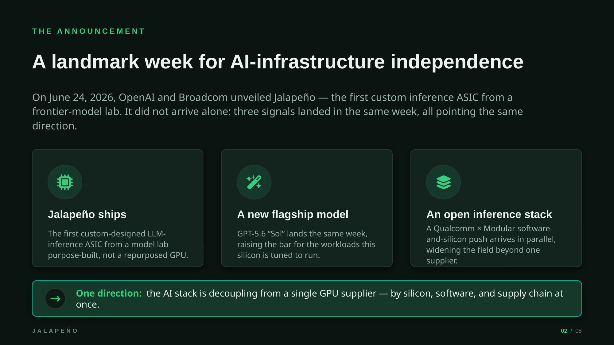
On June 24, 2026, a frontier AI developer and a major semiconductor partner unveiled the developer’s first custom inference chip: an application-specific integrated circuit (ASIC) designed from scratch to run large language models, rather than a general-purpose processor adapted to the job. The companies say the chip went from initial design to manufacturing tape-out in nine months - which they describe as possibly the fastest development cycle ever for high-performance, leading-edge silicon - and that early testing shows performance per watt substantially better than today’s best accelerators. The goal is blunt: cut the cost and power of running AI at the scale of billions of daily queries.
The slides embedded below are a ready-to-use deck on this same topic, generated by AskDeck from a short brief. The explanation continues here.
Why inference, not training, is the cost center
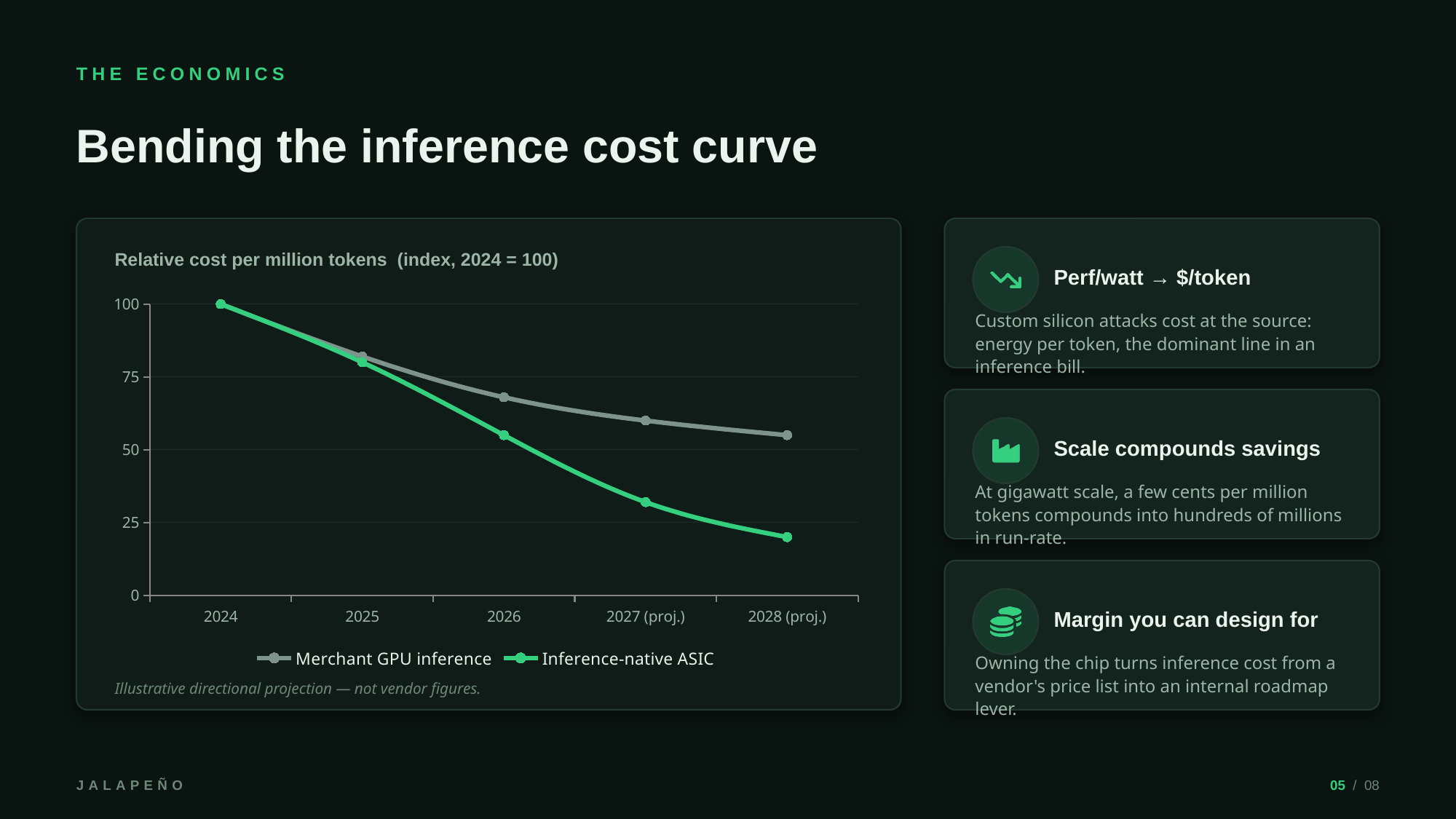
Training is the one-time, compute-heavy process of building a model. Inference is what happens every time someone uses it: the model reads a prompt and generates a response one token at a time. Inference is where AI reaches people, and because it runs on every single query, its cost compounds. Two numbers dominate the economics - performance per watt (how much useful work you get per unit of energy) and cost per token. Lower both and every product built on the model gets cheaper to run and faster to respond.
Why a purpose-built ASIC can beat a general-purpose GPU
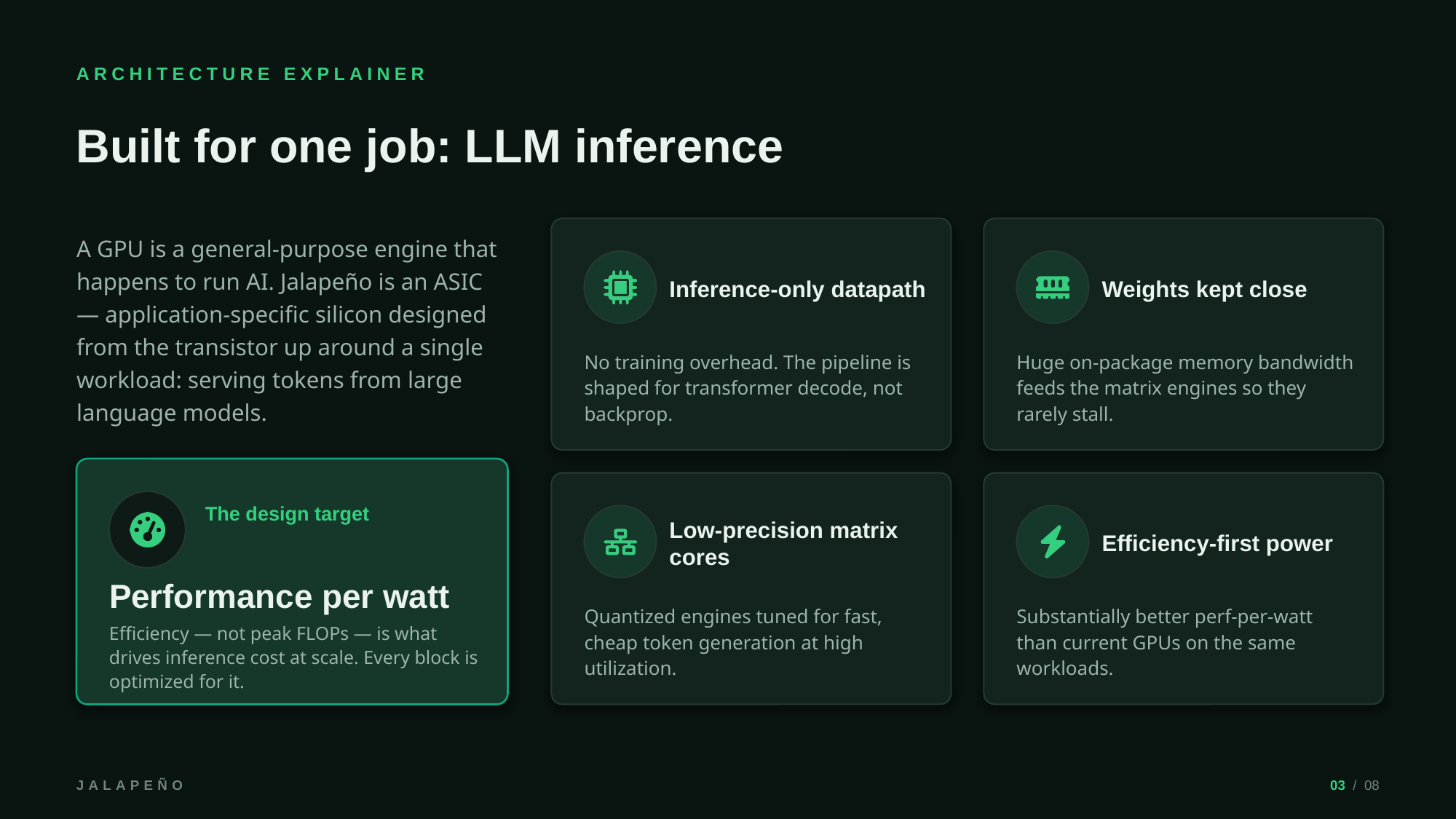
General-purpose GPUs were optimized for training: enormous floating-point throughput, many stacks of high-bandwidth memory, and data processed in parallel. Text generation works differently. The “decode” phase produces one token at a time in an autoregressive loop, and each step has to pull the model’s weights and the growing key-value cache out of memory. That makes decode memory-bandwidth bound - the chip spends more time waiting for data to arrive than doing math. Engineers have argued that the prevailing design, a large die packed with raw FLOPS, is a mismatch for this workload. A chip built only for inference can rebalance around the kernels, memory movement, and networking that LLM serving actually stresses, cutting data movement so real-world utilization lands closer to the hardware’s theoretical peak. That is where the efficiency gains come from.
What “tape-out in nine months” actually means
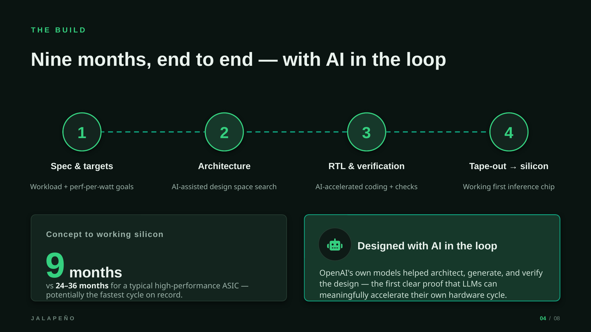
Tape-out is the milestone where a finished design is handed to a foundry to make photomasks and fabricate the first silicon. It matters because mistakes are expensive: a re-spin at an advanced node can cost well over $10 million, which is why verification typically eats 60 to 70 percent of a chip project’s effort, and complex chips often take 12 to 24 months just to reach silicon - longer at the leading edge. Doing it in nine months is unusual.
The other notable detail: the developer used its own AI models to speed up parts of the design and optimization. That is the first concrete sign that large language models can meaningfully accelerate the hardware that runs them. If AI can help engineers design better chips faster, the cost of compute could fall across the whole industry.
What it changes for AI costs and the silicon landscape
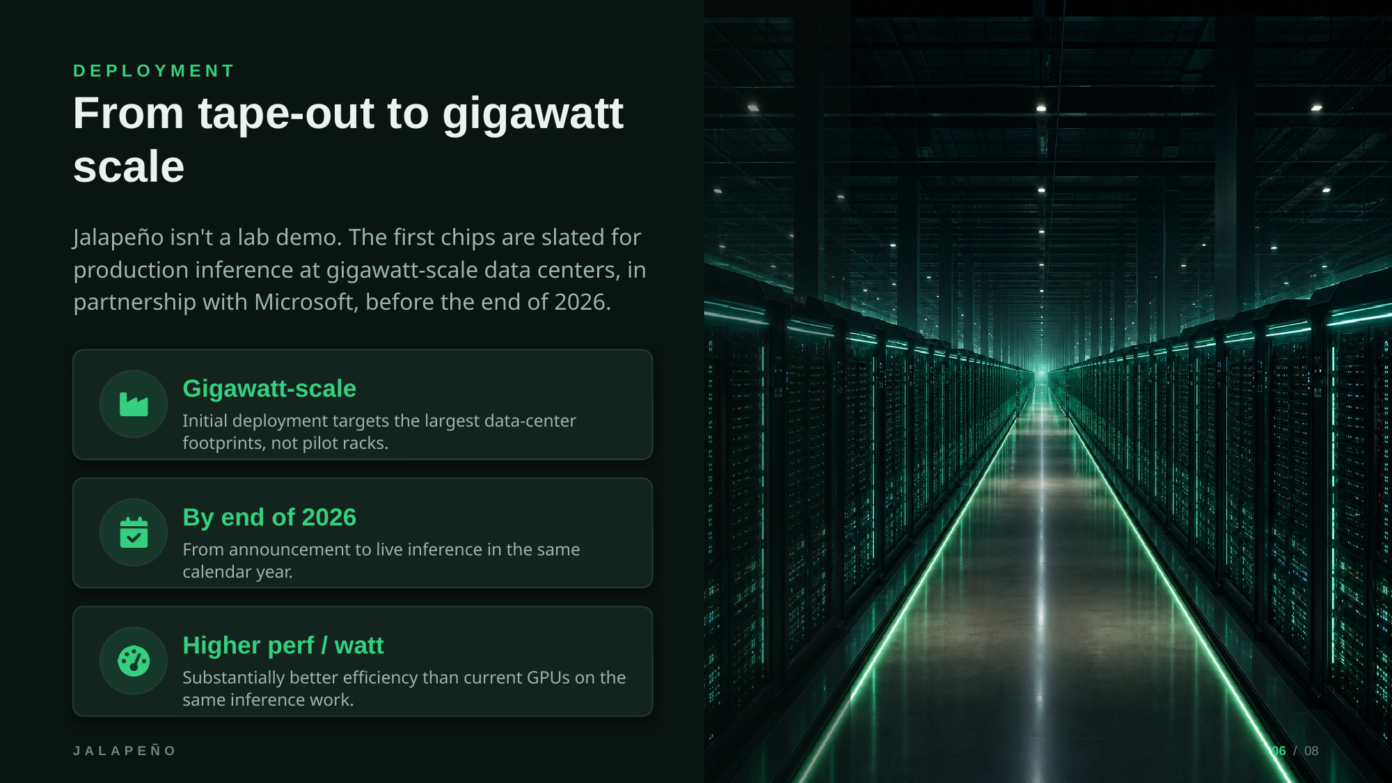
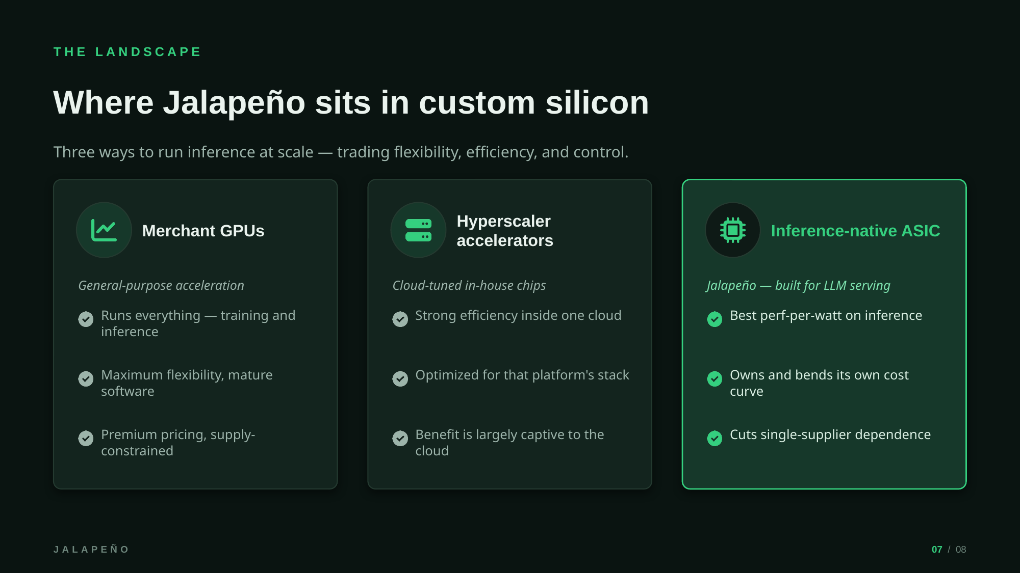
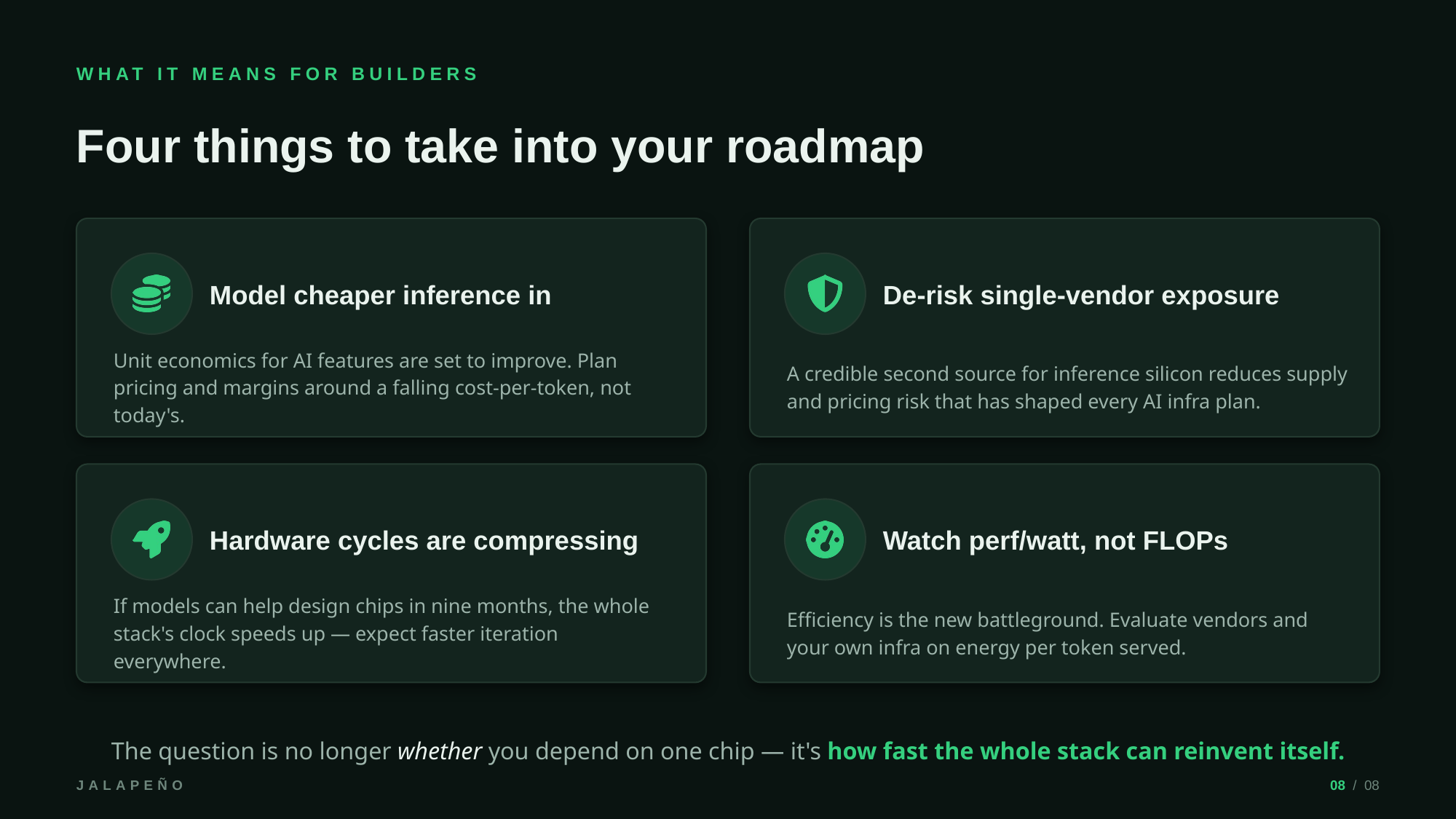
Custom AI silicon is not new. Large cloud operators have designed their own accelerators for years to avoid paying a premium for merchant GPUs and to tune hardware to their own workloads. What’s new is a model developer doing the same for inference specifically, as part of a full-stack push to design chips, kernels, serving systems, and models together. Engineering samples are already running real machine-learning workloads in the lab at production frequency and power, with initial deployment planned in gigawatt-scale data centers by the end of 2026 and a multi-generation roadmap behind it. For anyone building on these models, the takeaway is the cost curve: cheaper, more efficient inference means cheaper AI features and less exposure to a single chip supplier.
What is the difference between a training chip and an inference chip?
Training chips maximize raw parallel compute to build a model from data. Inference chips prioritize low latency, high memory bandwidth, and energy efficiency to serve a finished model to users. A chip tuned only for inference can drop features training needs and spend that silicon budget where serving actually bottlenecks.
Why is LLM inference memory-bound rather than compute-bound?
Generating text is sequential: the model produces one token, then uses it to produce the next. Each step reloads billions of parameters and the growing key-value cache from memory, so throughput is limited by how fast data moves, not by raw math. Prefill, where the prompt is read in parallel, is more compute-bound.
Will custom inference chips make AI cheaper?
That is the intent. Better performance per watt lowers the energy and hardware cost of each token, and more competition in accelerators reduces reliance on any one supplier. The real savings depend on production yields and deployment at scale.
The example deck below was built with AskDeck from a short brief and lays this story out across eight slides - the architecture, the nine-month timeline, and the cost picture. You can download it, edit any slide, and adapt it to your own audience.
See the deck